
Figure 1. TSV (Through-Silicon Via) formed vertically between semiconductor chips
As shown in Figure 1, TSV (Through-Silicon Via) technology in semiconductor processes is one of the core technologies that enables vertical connections between chips. TSVs improve space efficiency compared to conventional horizontal interconnects, reduce signal transmission time, and enhance energy efficiency. Measuring TSV depth is essential to ensure the accuracy and reliability of such vertical interconnect technologies. Precise depth measurement reduces defect rates in manufacturing processes, thereby lowering costs and improving yield and overall production efficiency.
The t-Nova-1550R from Meterlab is well suited for this important TSV depth-measurement task. The t-Nova-1550R is based on a spectrally resolved interferometer and is designed to meet various measurement requirements in semiconductor processing. In particular, for TSV depth measurement the t-Nova-1550R offers several distinctive and important advantages over conventional instruments.
Using the principle of spectral interferometry, the t-Nova-1550R enables nanometer-scale high-resolution measurements, allowing very precise determination of TSV depth and diameter. As an optical, non-destructive measurement method, it permits repeated measurements and real-time process monitoring without damaging samples, thus reducing sample loss in production. With a high measurement speed of 40 kHz, it can rapidly perform TSV inspection and quality control in mass-production environments, improving manufacturing throughput. In addition, by operating in the near-infrared wavelength band, it can be applied to measure a variety of semiconductor samples, including those containing silicon.
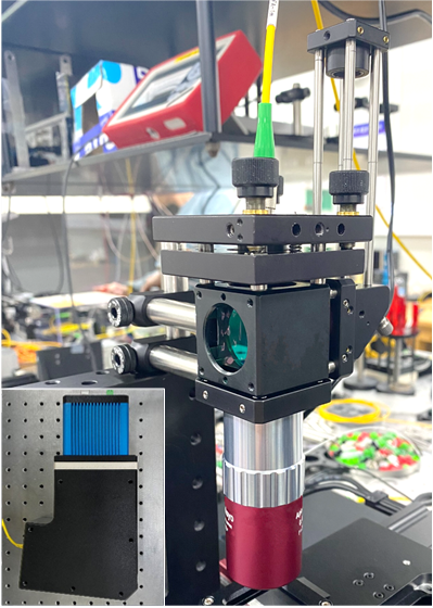
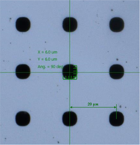
Figure 3. TSV sample with nominal diameter 5 μm and nominal depth 50 μm and the measurement location
Figure 2 shows the experimental setup of the t-Nova-1550R implemented using the s-Nova-1550 for TSV measurement. Using this setup, we measured the depth of a TSV whose nominal diameter and depth are 5 μm and 50 μm, respectively — a TSV with a relatively large aspect ratio of about 1:10. For the TSV sample shown in Figure 3, the measured actual depth was 40.497 μm, and this result agreed with validation values from other equipment within 80 nm.
In this way, Meterlab’s t-Nova-1550R, combining a high-speed spectrometer s-Nova-1550 with high-precision TSV measurement capability, is expected to be widely applied as a real-time monitoring tool for TSV depth measurement in semiconductor manufacturing processes.