[t-Nova Series - Applications]
In devices for semiconductors, batteries, and displays, various thin films of different materials are used. Among these materials, metals with high electrical conductivity are used in metallization processes to form electrodes and circuit patterns that electrically control and connect devices. Commonly used metals include aluminum (Al) and copper (Cu), which are deposited as thin films with thicknesses on the order of nanometers. As with other films formed within a device, measurement of the metal film thickness — which determines electrical performance and yield — is necessary for process control.
Among the t-Nova series, the t-Nova-525R (prototype) is a visible-band spectroscopic reflectometry sensor that can measure thin films down to a few nanometers. The t-Nova-525R is capable of measuring not only transparent non-metallic materials or non-metallic compounds in the visible band but also opaque metals with high precision.
In general, metals are considered difficult to measure with some optical methods because light does not penetrate deeply into metals. However, when a metal film is extremely thin (a few nanometers), light can penetrate through the film and the light reflected from the lower interface can be collected to enable thickness measurement. Unlike thick films, metal thin films can be measured in the visible band because their penetration depth is typically on the order of tens of nanometers or less, depending on the metal material.
Penetration depth: a physical quantity indicating how deeply electromagnetic radiation (light or other EM radiation) can penetrate into a medium.
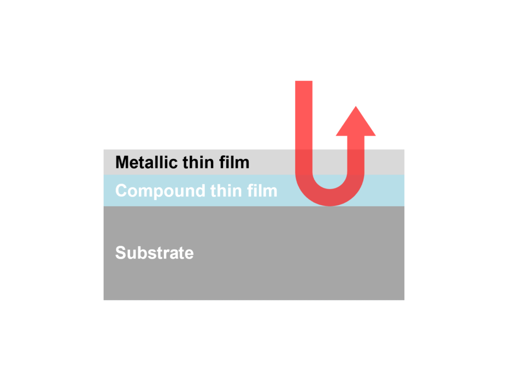
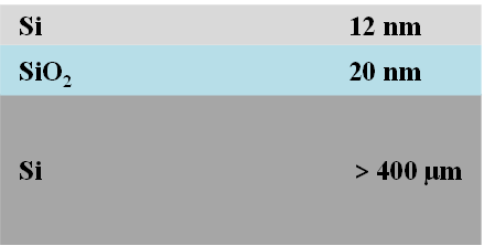
Figure 1. the structure of a metal thin-film sample
Figure 1 shows the structure of a metal thin-film sample measured using the same principle as the t-Nova-525R visible spectroscopic reflectometer. A silicon (Si) substrate (a metalloid) is present beneath the thin film, and a silicon oxide (SiO2) layer exists between the substrate and the film.
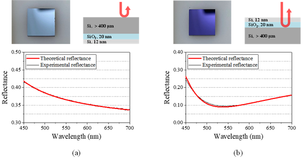
Figure 2. (a) Thick metal film; (b) Measurement conditions and reflectance spectra for metal thin films

Table 1. Thickness measurement results for metal thick films and thin films
Figure 2 presents the physical samples, a schematic of the measurement light, experimental and theoretical reflectance spectra obtained using a visible spectroscopic reflectometer, and Table 1 summarizes the thickness measurement results under the conditions in Figures 2(a) and 2(b). For a thick metal film, as in Figure 2(a), the measurement light is reflected only from the top surface of the sample, making it impossible to measure the thicknesses of all layers (see Table 1). In contrast, for a sufficiently thin metal film (Figure 2(b)), light transmits into the sample and it is possible to measure not only the metal thin film but also the thickness of the underlying silicon oxide layer.
Thanks to the visible spectroscopic reflectometry principle implemented in Meter-Lab’s t-Nova-525R, we expect this sensor to be widely applicable for thickness measurements of a broad range of thin films used in advanced devices — including non-metals, metals, and various compounds.