Flux is a chemical substance used in semiconductor packaging, particularly in soldering and reflow processes, to remove oxide layers from metal surfaces and improve solder wettability at the bonding interface. Since flux must be uniformly applied across wafers or substrates to ensure reliable electrical and mechanical connections between solder balls and pads, it is considered an essential material in semiconductor assembly processes.
Flux thickness can vary depending on the application method—such as spraying, dipping, or stencil printing—and even small thickness variations can result in defects in the final product. If the flux layer is too thick, excessive residue may remain after processing, potentially leading to void formation within the solder joint. Conversely, if the flux layer is too thin, oxide layers may not be sufficiently removed, resulting in unstable bonding and potentially causing open-circuit defects. As a result, flux thickness is a critical process parameter that must be carefully controlled, as both excessive and insufficient thickness can negatively affect product quality. For this reason, accurately monitoring flux thickness and distribution at an early stage of the process has become increasingly important for improving yield and ensuring product reliability. In particular, the ability to capture the thickness distribution across the entire wafer surface immediately after application is essential for identifying localized variations that could otherwise go unnoticed.
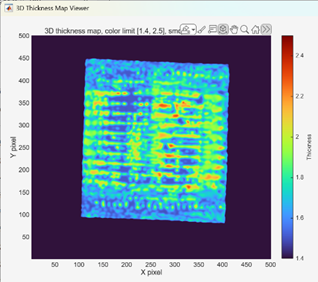
Figure 1. Measurement Results
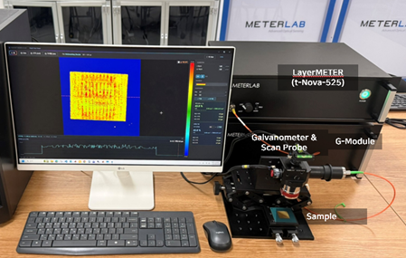
Figure 2. Measurement System
MeterLab provides a solution for precise, non-contact flux thickness measurement in semiconductor packaging processes through the combination of the FilmMETER (t-Nova-525R) and G-Module. The system provides a measurable thickness range of 50 nm to 200 µm, enabling a single system to measure both ultra-thin films and relatively thick flux layers. Measurement speeds of up to 250 kHz allow rapid data acquisition that can keep pace with high-throughput production environments. In addition, area scanning with the G-Module supports measurement areas of up to 20 × 20 mm, making it suitable for evaluating thickness distribution over a wide surface area.
The combination of these capabilities enables rapid scanning across a wide thickness range—from ultra-thin films to thick flux layers—while generating a near-real-time thickness distribution map suitable for inline process monitoring. A key advantage of the system is that it not only measures thickness at a single point but also visualizes thickness distribution across the entire wafer or substrate surface. This capability allows users to detect equipment setup issues and localized process variations at an early stage. As a result, process deviations can be identified and corrected promptly, helping reduce defect rates and improve overall manufacturing productivity.
Accurate measurement and control of flux thickness are critical factors in ensuring the reliability of semiconductor packaging processes. MeterLab’s FilmMETER and G-Module deliver three key capabilities—a wide thickness measurement range, high-speed measurement, and large-area scanning—providing a practical solution for process monitoring and quality control in semiconductor manufacturing environments.
