[t-Nova Series - Applications]
In advanced devices across fields such as semiconductors, batteries, and displays, multilayer structures with numerous thin films—ranging from tens to hundreds of nanometers in thickness—are widely used on thick substrates. Depending on their intended function, multilayered films exhibit different optical, electrical, and chemical properties according to their thickness and uniformity, and these properties are critical factors determining device performance. Accordingly, many manufacturing processes require measurement of multilayer film thickness and uniformity for quality control and yield improvement. In particular, there is strong demand for real-time monitoring technologies that can be applied inline in production processes.
Meter-Lab’s t-Nova series, a family of high-precision optical thickness sensors, offers multiple models capable of measuring from tens of nanometers to several millimeters. Among them, the prototype shown in Figure 1, the t-Nova-525R, is a reflection-type sensor optimized for measuring thin-film samples with thicknesses from tens to hundreds of nanometers using visible light centered at 525 nm.
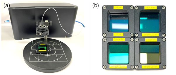
Figure 1. (a) Prototype of t-Nova-525R (under development) and (b) multilayer (≤3 layers) thin-film samples.
The t-Nova-525R implements the principle of spectroscopic reflectometry, which enables the fastest, high-precision measurement of films thicker than several tens of nanometers among current optical thin-film metrology techniques. Using this approach, we achieved real-time multilayer thin-film thickness measurement with sub-nanometer precision, as shown in Video
Video 1. Real-time multilayer thin-film thickness measurement using the t-Nova-525R.
Figure 2 shows images of the three thin-film samples measured in Video 1, acquired with a scanning electron microscope (SEM), the most commonly used electronic inspection instrument in industry for observing fine sample morphology and structure. Table 1 lists the per-layer thickness measurements obtained by the t-Nova-525R and the deviations from the SEM measurements. The SEM measures film thickness by imaging a cut cross-section of the sample and can provide only the total thickness without distinguishing individual layers. In contrast, the t-Nova-525R performs non-destructive, real-time measurements and, as shown in Table 1, yields measurements similar to SEM while also distinguishing layer-by-layer thicknesses.
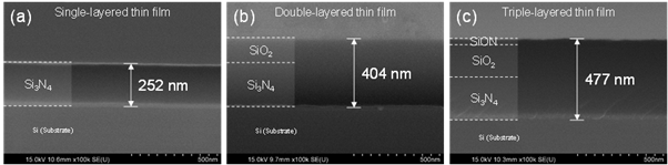
Figure 2. SEM images of the three thin-film samples: (a) single-layer sample, (b) two-layer sample, (c) three-layer sample.
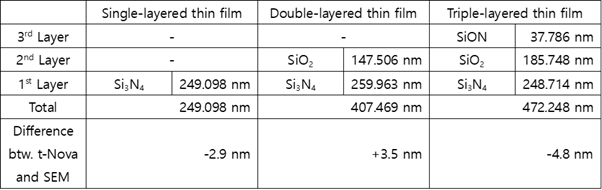
Table 1. Per-layer thickness measurements by t-Nova-525R and deviation from SEM measurements.
With its high precision and high-speed multilayer thickness measurement capability, the t-Nova-525R from Meter-Lab is expected to be widely applicable to manufacturing processes of various advanced devices that require real-time multilayer thin-film thickness monitoring.