[t-Nova Series - Applications]
Wafers used as substrates for forming semiconductor integrated circuits are typically made of silicon. To reduce defects in the circuits formed on wafers, a high degree of thickness uniformity across the wafer is required, and therefore real-time monitoring via high-speed thickness measurement is necessary. Optical thickness metrology is commonly used in semiconductor processes for high-speed, high-precision thickness measurement; among these methods, optical interferometry is a representative technique. Interferometric methods are non-contact and can measure optical thickness with nanometer (nm)-level precision in millisecond (ms) timescales without damaging the wafer surface.
To measure silicon thickness using interferometry, as illustrated in Figure 1, one must detect not only the light reflected from the top surface of the silicon but also the light that transmits through the silicon and reflects from its bottom surface. Therefore, an illumination wavelength capable of transmitting through silicon must be used. Meter-Lab’s t-Nova-1550R, a reflection-type high-precision optical thickness sensor, employs light with a center wavelength of 1550 nm and can measure silicon thicknesses from 1 μm to 1.2 mm (assuming refractive index n ≈ 3.6).
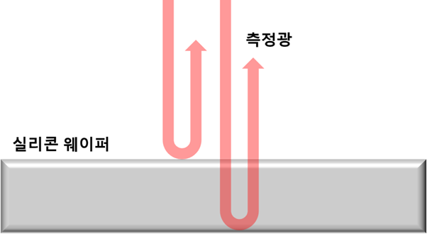
Figure 1. Measurement geometry showing the illumination required for silicon wafer thickness measurement
Figure 2 shows the experimental setup for silicon thickness-profile measurement using the t-Nova-1550R. The setup is compact: a small, lightweight t-Nova-1550R probe (30 mm diameter, 60 mm length) is positioned at a working distance of 60 mm from the sample, and the sample is a 480 μm thick silicon wafer mounted on a stage capable of lateral translation.
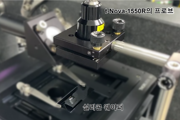
Figure 2. t-Nova-1550R setup for silicon thickness measurement
Video 1. t-Nova-1550R silicon wafer thickness-profile measurement
As shown in Video 1, while translating the silicon wafer, we acquired a thickness profile over a 40 mm region at high speed (tens of kHz) with nanometer-level precision. With its combination of high speed and high precision, Meter-Lab’s t-Nova-1550R is expected to be widely applicable to various semiconductor manufacturing processes that utilize silicon wafers.